 en
en fr
fr de
de zh
zhNPS300
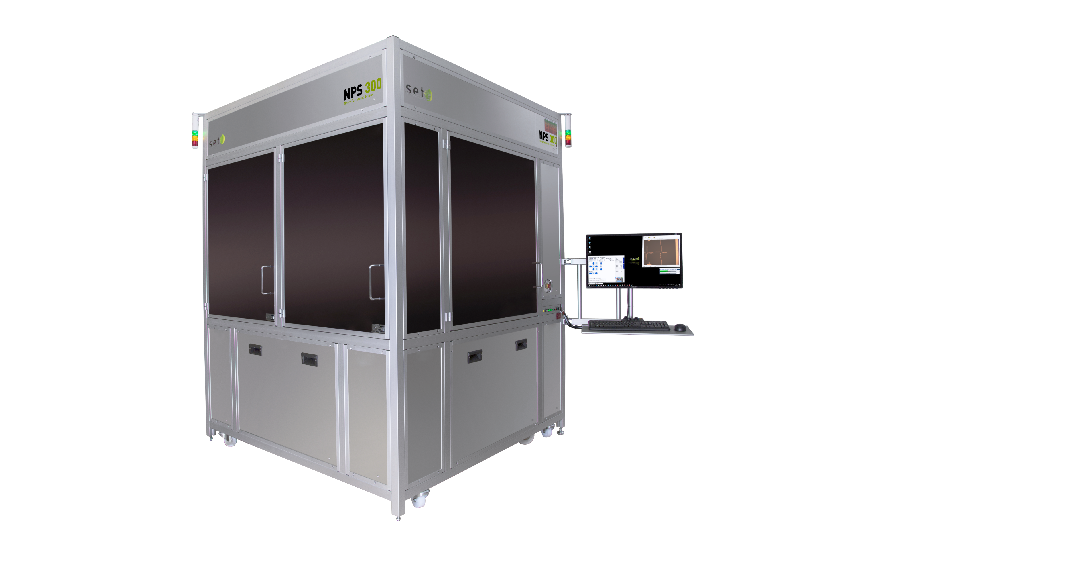
Advanced R&D and pilot line oriented, the NPS300 is a high accuracy and high force Stepper designed for nano-imprinting.
Optimized for replication of nanostructures with ± 0.5 μm accuracy, the NPS300 is the first ever tool able to combine aligned Hot Embossing Lithography and UV-NIL on a same platform.
The NPS300 is able to print sub-20 nm geometries with an overlay accuracy of 250 nm.
Its flexible architecture offers an excellent process reproducibility and a unique ability to pattern large areas, in a sequential Step & Repeat mode on wafers up to 300 mm.
It enables the low cost manufacturing of large stamps featuring repeated patterns.
000
Key benefits
- ± 0.5 μm accuracy
- Step & Repeat mode on wafer up to 300 mm
- Automatic stamp pick-up
- Air bearing technology and granite structure ensuring long-term stability and reliability
- Control of parallelism to guarantee very high accuracy even under high forces
- Hand free/full automated calibration
- Automatic cycle and operator independent
- High yield thanks to a stiff design
- Process recording for development, log files to track production
Process capabilities
The Step & Stamp Imprinting Lithography for Hot Embossing or UV-NIL is an innovative method that has been demonstrated at the VTT Technical Research Centre of Finland.
- Hot Embossing Lithography: this method consists of transferring the stamp pattern into a thermoplastic embossing material by controlling heat and pressure
- UV-NIL: the Step & Cure method is using in-situ imprinting material dispensing and UV curing. This cutting-edge technology is a very promising solution for replacing standard UV-lithography systems when sub-20 nm resolution is required.
Applications
- Photonic devices
- High precision micro-optical arrays and gratings
- High resolution OLED displays
- Large stamp creation
- Other emerging techniques
NIL technology
Low cost production solutions of nanostructures are in development that may be the driving forces of Semiconductor, MOEMS and optoelectronics technology tomorrow. In particular, NanoImprint lithography (NIL) and its variations have been developed as a cost-effective alternative to high-resolution e-beam lithography to print sub-20 nm geometries.
Imprinting is based on the principle of mechanically pressing thin polymer film with a stamp containing the nanopattern, in a thermo-mechanical or UV curing process. The patterned polymer can act as a final device, e.g. lense for imaging sensors, micro fluidic chip, biomedical array etc. It can also be used as a high resolution mask for subsequent steps of the process.
Imprinting is a straightforward lithography technology. There are three basic process steps:
- Align the stamp with the substrate which has been pre-coated with the imprinting material
- Press the stamp into the imprinting material to transfer the pattern written on the stamp surface
- Separate the stamp from the imprinting material
We can describe three imprinting or embossing techniques: Hot Embossing Lithography (HEL) using thermal plastic material, UV-NIL using a liquid resist which is then cured with UV light after molding and Soft Lithography which transfers ink previously applied to a soft stamp onto a substrate using a stamping method.
Technical data
Click here to request the NPS300 datasheet.