 de
de zh
zh en
en fr
frDirect Bonding
Process
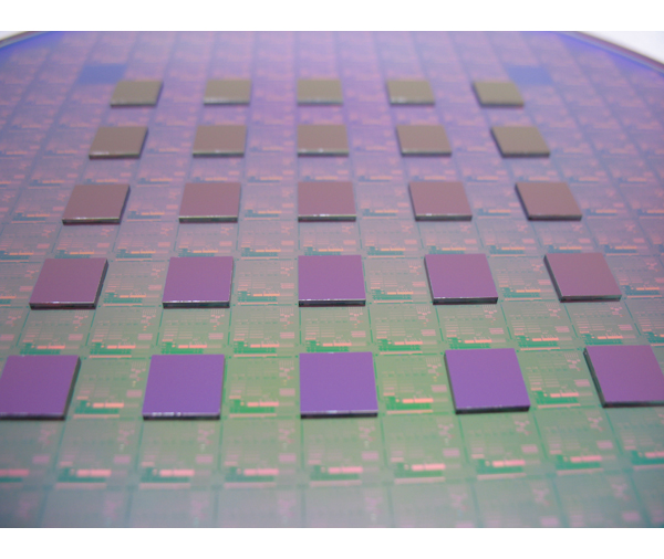
Direct / Hybrid Bonding, used to assemble two components, offers three main advantages:
- Low bonding force
- Bonding process at room temperature
- Short process cycle
However, it presents one challenge for the bonding step: components must have a very high level of cleanliness.
Technology benefits
The bonding process requires low force and room temperature. It enables high accuracy bonding for high density interconnections by circumventing thermal expansion of different materials.
To ensure void-free bonding, the alignment and bonding steps must take place in a particle-free environment. It is accomplished by the use of special materials and careful management of air flow.
All these advantages permit to reach a high throughput required for widespread adoption of 3D Integration.
A long experience
SET successfully demonstrated the feasibility of Die-to-Wafer approach using Direct / Hybrid Bonding, with an accuracy < 1μm, thanks to a specially designed FC300. This success was the subject of numerous articles.
At the end of 2015, SET joined the IRT Nanoelec to design a rapid high accuracy Flip-Chip Bonder dedicated to Direct / Hybrid Bonding. Capitalizing on the experience of the PROCEED Project, SET designed and developed the NEO HB for production.
In 2019, SET launched the NEO HB at SEMICON Taiwan, thus meeting the high throughput needs necessary for widespread adoption of 3D Integration.